electronics
Circuit topologies and measured behavior: filters, semiconductors, op-amps, oscillators, feedback, conversion, and FPGA logic.
passive networks · diodes · transistors · op-amps · oscillators & modulation · sensing & control · audio · ADC & DAC · digital logic & FPGAs · physical limits
topology→operating region→transfer behavior→loading + limits
Reading rule. A schematic fixes connectivity; the component model fixes local behavior; feedback and loading fix the realized transfer. Every figure below pairs a circuit with the voltage, waveform, spectrum, or state it produces.
Passive networks: division, filtering & resonance
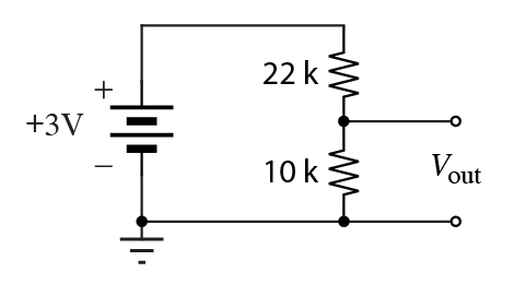
Voltage divider. \(V_{\rm out}=V_{\rm in}R_2/(R_1+R_2)\). Seen from the output, \(V_{\rm th}=V_{\rm out}\) and \(R_{\rm th}=R_1\parallel R_2\); with load \(R_L\), replace \(R_2\) by \(R_2\parallel R_L\).
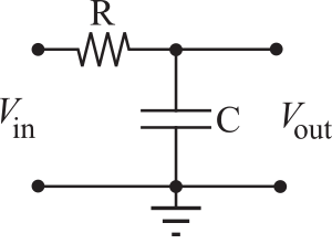
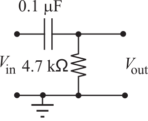
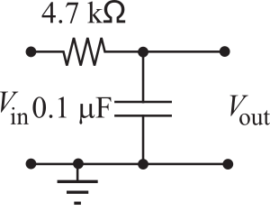
Capacitor dynamics. \(I=C\,\dd V/\dd t\), \(Z_C=1/(i\omega C)\), and \(\tau=RC\). A low-pass has \(H_{\rm LP}=1/(1+i\omega RC)\); a high-pass has \(H_{\rm HP}=i\omega RC/(1+i\omega RC)\). Both turn at \(f_c=1/(2\pi RC)\), where the gain is \(1/\sqrt2\) and the asymptotic slope is \(20\,\mathrm{dB/decade}\).
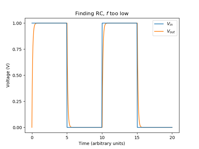
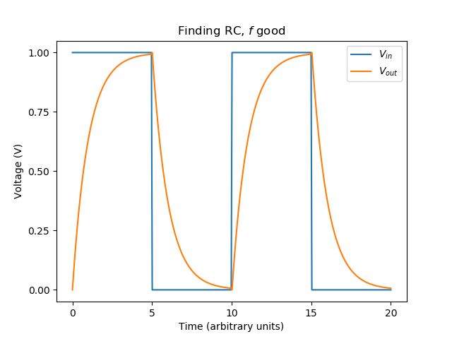
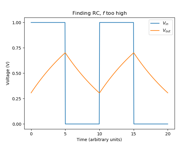
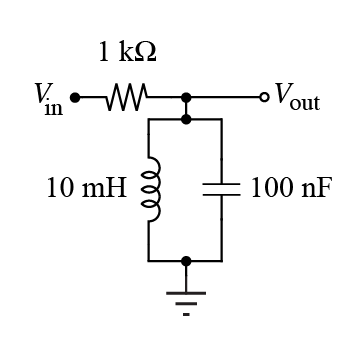
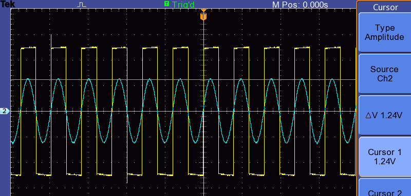
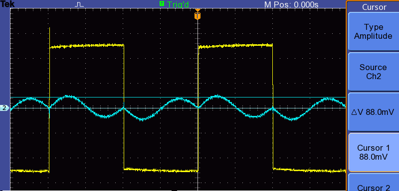
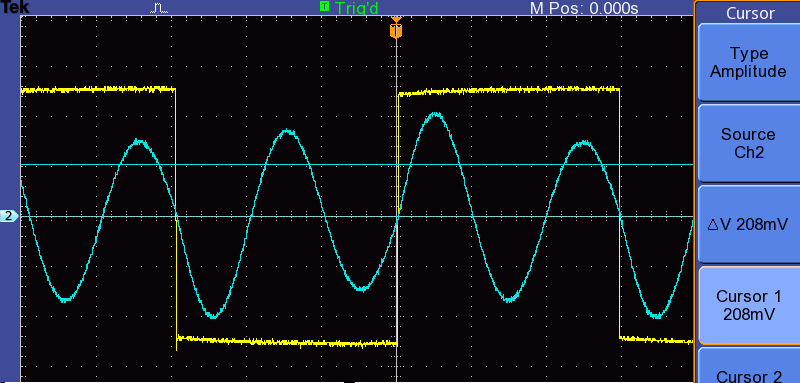
Resonance. \(f_0=1/(2\pi\sqrt{LC})\). The half-power points satisfy \(|V|=|V|_{\max}/\sqrt2\); \(Q=f_0/\Delta f\). Higher \(Q\) gives narrower selection and longer ringing. A square wave contains odd harmonics, so shifting the drive frequency moves successive harmonics through the same resonance.
Diodes: one-way, piecewise nonlinear behavior
Piecewise silicon model. The diode is open while \(V_A-V_K\lt V_D\), and conducting with nearly fixed \(V_A-V_K\approx V_D\) once on; \(V_D\) is commonly about \(0.6\,\mathrm V\) but depends on device, current, and temperature. Always include a resistor or other impedance that limits forward current.
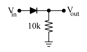
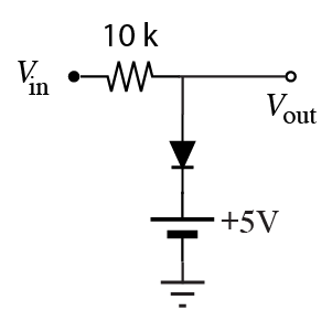
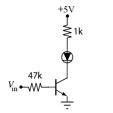
Clamp and protection. A diode to \(V_{\rm ref}\) limits \(V_{\rm out}\) near \(V_{\rm ref}\pm V_D\); the series resistor absorbs the excess voltage and limits clamp current. Reverse the diode to reverse the clipped polarity. LEDs obey the same current-limit requirement: \(R=(V_{\rm supply}-V_F)/I_{\rm LED}\).
Transistors: switching, buffering & gain
| NPN regime | First-order condition | Circuit meaning |
|---|---|---|
| cutoff | \(V_{BE}\lt0.6\,\mathrm V,\ I_C\approx0\) | open switch |
| forward active | \(V_{BE}\approx0.6\,\mathrm V,\ I_C\approx\beta I_B,\ V_C\gt V_B\) | controlled current / analog gain |
| saturation | load prevents \(\beta I_B\); \(V_{CE}\) small | closed switch |
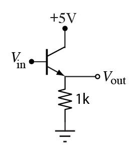
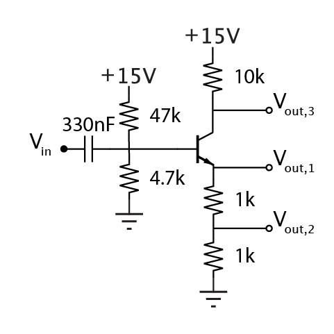
Active-region amplifier. Bias the transistor so the whole waveform stays between cutoff and saturation. With collector resistor \(R_C\) and unbypassed emitter resistance \(R_E\), \(A_v\approx-R_C/R_E\): increasing base voltage raises current, increasing the drop across \(R_C\), so collector voltage falls.
Current driver. A control signal supplies only base or gate drive; the load current comes from the load supply. A flyback diode is mandatory across inductive loads. For MOSFETs, gate threshold is not the fully-on voltage: check \(R_{DS(on)}\) at the available gate drive, current, switching loss, and thermal resistance.
Operational amplifiers: feedback creates functions
Ideal negative-feedback rules. \(I_+=I_-=0\), and while the output remains unsaturated \(V_+\approx V_-\). The open-loop relation \(V_{\rm out}=A(V_+-V_-)\) has enormous \(A\); negative feedback moves the output until the input difference is nearly zero.
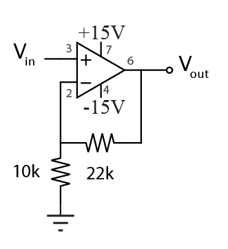
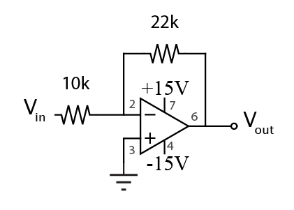
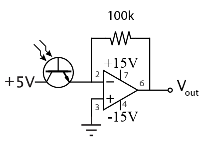
| Feedback network | Ideal function |
|---|---|
| output directly to (-) | follower: \(V_{\rm out}=V_{\rm in}\) |
| several \(V_i\) through \(R_i\) to (-) | summer: \(V_{\rm out}=-R_f\sum_iV_i/R_i\) |
| matched ratios on both inputs | difference: \(V_{\rm out}=G(V_2-V_1)\) |
| sensor current into (-) | transimpedance: \(V_{\rm out}=-I_{\rm in}R_f\) |
| capacitor in feedback | integrator: \(V_{\rm out}=-(R_{\rm in}C)^{-1}\int V_{\rm in}\,\dd t\) |
| capacitor at input | differentiator: \(V_{\rm out}=-R_fC\,\dd V_{\rm in}/\dd t\) |
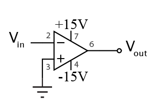
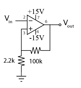
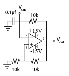
Hysteresis and oscillation. If feedback returns a fraction \(\alpha\) of symmetric \(\pm V_{\rm sat}\), thresholds are \(\pm\alpha V_{\rm sat}\). With an RC charging path, \[f=\left\{2RC\ln\!\left(\frac{1+\alpha}{1-\alpha}\right)\right\}^{-1}.\]
Real limits. Output swing stops near the rails; input common-mode range is finite; output current, gain-bandwidth, slew rate \(\max|\dd V_{\rm out}/\dd t|\), bias current, and offset are finite. Once a demanded output violates any limit, \(V_+\approx V_-\) no longer applies.
Oscillators, duty cycle & modulation
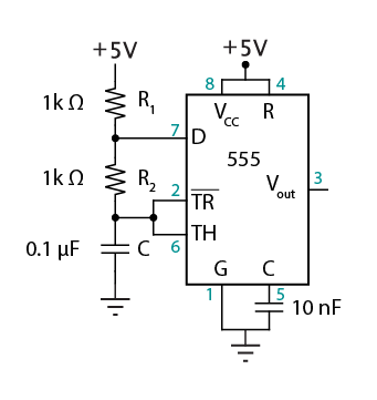
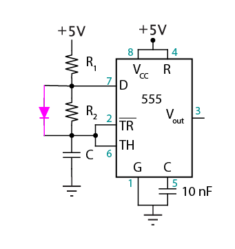
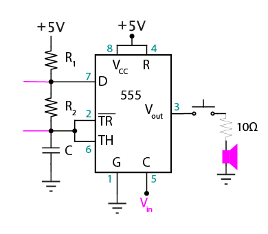
Standard timing. \[t_H=\ln2\,(R_1+R_2)C,\qquad t_L=\ln2\,R_2C,\qquad f=\frac{1}{\ln2\,(R_1+2R_2)C}.\] The ordinary topology therefore spends more than half its period high.
Sensing & closed-loop control
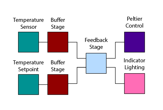
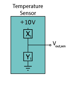
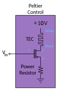
Thermistor. For an NTC device, resistance decreases with temperature: \[R(T)=R_0\exp\!\left[\beta\left(\frac1T-\frac1{T_0}\right)\right].\] Put the thermistor in the upper or lower divider leg to select the sign of \(\dd V_{\rm sense}/\dd T\). Define \(e=V_{\rm set}-V_{\rm sense}\), then confirm the total loop sign is negative: a temperature rise must eventually command less heating or more cooling.
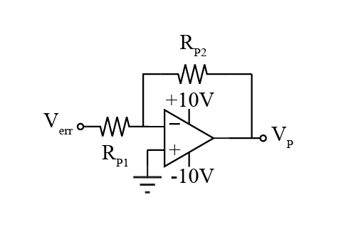
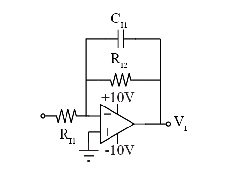
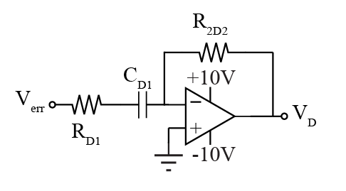
PID law. \[u(t)=K_Pe(t)+K_I\int e(t)\,\dd t+K_D\frac{\dd e}{\dd t}.\] P responds immediately but leaves finite error; I removes persistent offset but can wind up; D anticipates motion and adds damping but amplifies high-frequency noise.
Audio as a complete analog signal chain
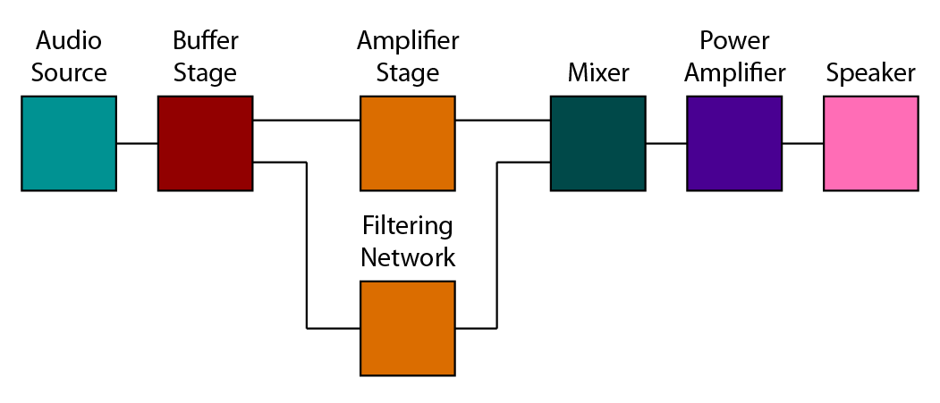
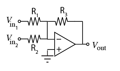
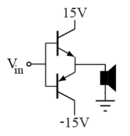
Impedance and power. A small-signal op-amp can produce the correct unloaded voltage yet current-limit into an \(8\,\Omega\) speaker. Buffers isolate high-impedance signal stages from low-impedance loads. Class-AB bias reduces the roughly \(1.2\,\mathrm V\) dead band at the cost of idle current and heat.
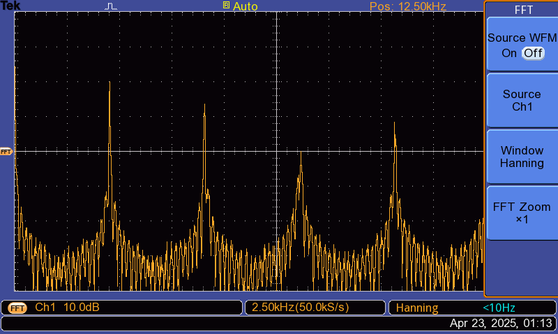
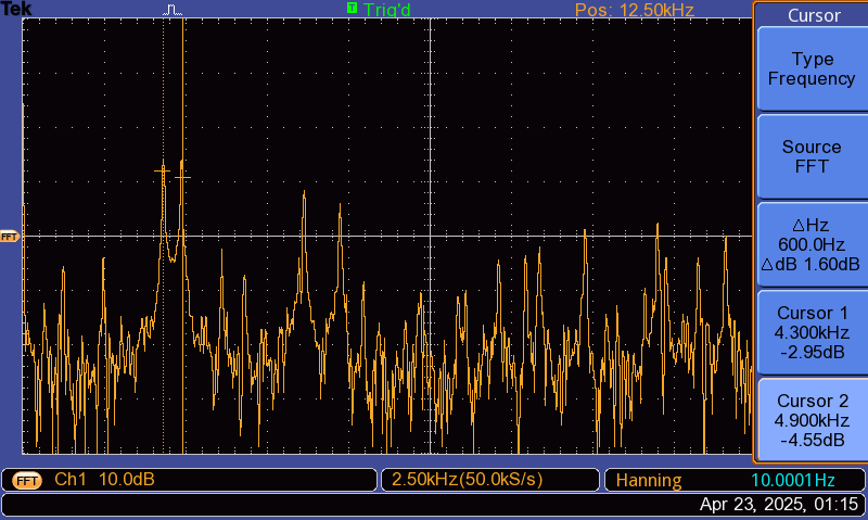
Spectrum. Filtering changes tone by weighting harmonics; clipping creates new high-frequency components. Equal voltage does not imply equal loudness because speaker and hearing response are frequency dependent.
Analog ↔ digital conversion
Quantization. An ideal \(N\)-bit converter divides \(0\) to \(V_{\rm ref}\) into \(2^N\) codes. One LSB is \(\Delta V=V_{\rm ref}/2^N\), ideal quantization error is at most \(\Delta V/2\), and code \(D\) represents about \(DV_{\rm ref}/2^N\). Accuracy, offset, linearity, noise, and conversion time are separate limits.
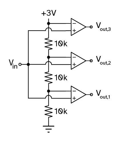
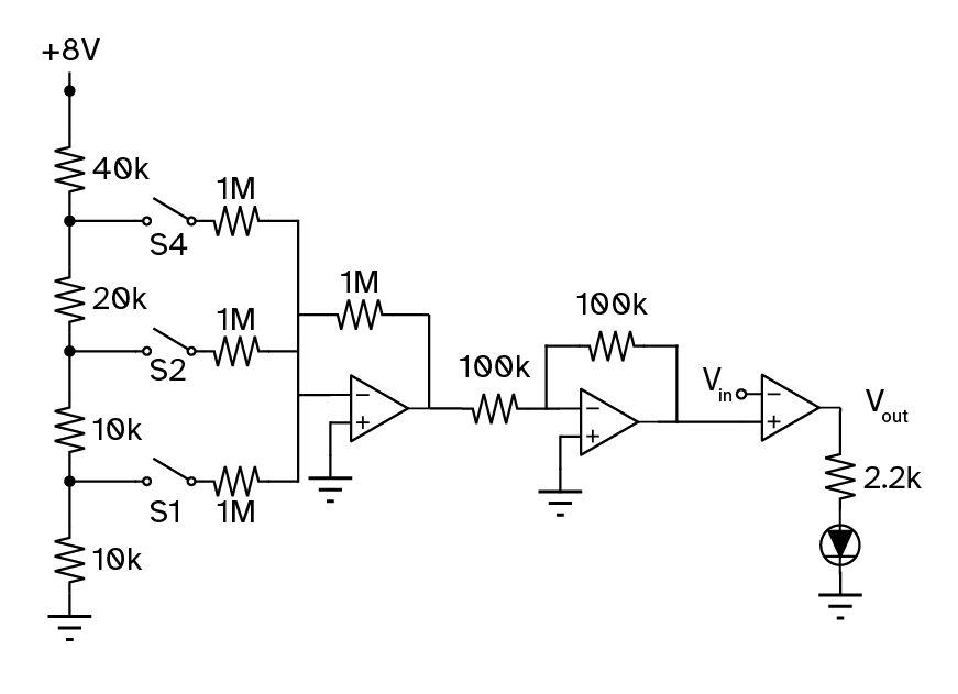
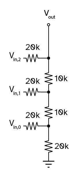
Digital interface. Parallel data exposes every bit simultaneously; serial data trades pins for protocol and latency. Logic thresholds are ranges, not ideal points: common \(5\,\mathrm V\) TTL treats inputs below \(0.8\,\mathrm V\) as LOW and above \(2.0\,\mathrm V\) as HIGH, but \(3.3\,\mathrm V\), \(1.8\,\mathrm V\), and CMOS families differ.
PWM as conversion. Switching between \(V_L\) and \(V_H\) with duty \(D\) gives average \(\bar V=DV_H+(1-D)V_L\). A low-pass or inertial load extracts the average; switching ripple and load current still require a filter and driver.
Digital logic & FPGAs
Hardware state. Combinational gates depend on present inputs; flip-flops capture state on a clock edge. In an FPGA, independent logic operates concurrently: counters, filters, interfaces, and state machines are spatial circuits, not instructions time-shared on one CPU core.

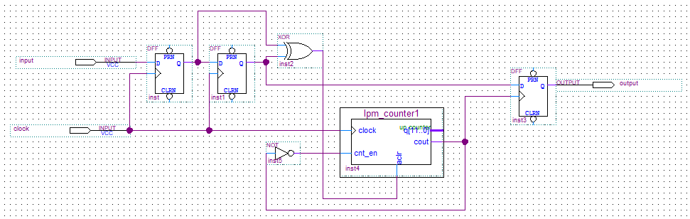
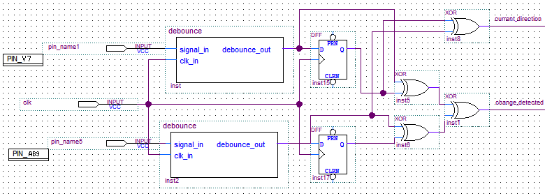
Physical I/O. A logical pin name has no electrical meaning until assigned to a package pin and I/O bank. Buttons and displays may be active-low; external logic must satisfy the bank's voltage, current, setup/hold, and asynchronous-input requirements.
Physical limits & observed behavior
Loading. A source with Thévenin pair \(V_{\rm th},R_{\rm th}\) driving \(R_L\) produces \(V_L=V_{\rm th}R_L/(R_{\rm th}+R_L)\). A \(50\,\Omega\) function generator, scope probe capacitance, next amplifier, or speaker is part of the circuit once connected.
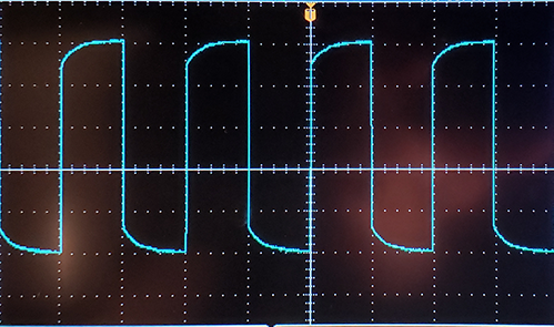
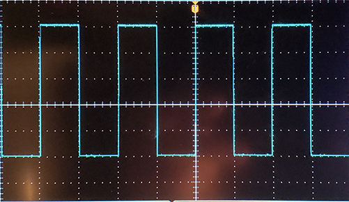
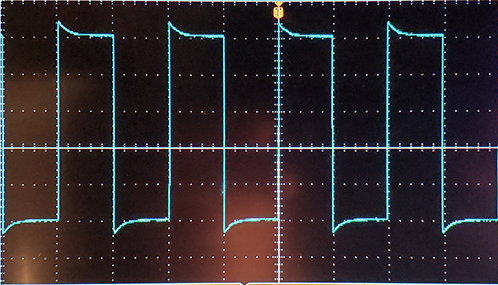
Edges reveal hidden dynamics. A nominal square wave contains arbitrarily high harmonics; real bandwidth, slew rate, stray capacitance/inductance, and transmission-line reflections round or ring its edge. Even the probe has an RC divider that must be compensated.
| Observed behavior | Likely physical cause |
|---|---|
| amplitude falls when connected | loading, source resistance, output-current limit |
| output sticks at a rail | wrong feedback sign, invalid common-mode input, demanded swing beyond rails |
| rounded or triangular large signal | bandwidth, slew-rate, or RC limit |
| overshoot, ringing, oscillation | phase margin, stray \(L/C\), long return path, probe ground inductance |
| works unloaded but not into actuator | supply sag, heat, shared-ground drop, current or power rating |
| digital transitions multiply | contact bounce, asynchronous sampling, undefined threshold, noise |
Datasheet boundary. Exact package and pinout; recommended operating conditions; absolute maximums; input/output voltage and current; output swing; common-mode range; bandwidth, slew, and switching time; thermal resistance; guaranteed min/max. Typical curves explain behavior but do not guarantee it.
Circuit figures and measured traces are from the UChicago PHYS 226 electronics laboratory; course logistics and apparatus-specific instructions are omitted.